Showing posts with label Arduino. Show all posts

12 June 2026

Simulating ADF ISB Transmissions: 12-Bit Repetition Coding on the USB Channel

The idea for this post stems from an interesting RAN (Royal Australian Navy) fleet broadcast originating from the MHFCS (Modernised High Frequency Communications System) utilized by the ADF (Australian Defence Force). The captured transmission employs STANAG-4285 at 600 bps/L in ISB (Independent SideBand) mode on 14874.0 kHz (Figure 1), and was successfully recorded thanks to the remote KiwiSDR VK6QS2 located in Augusta, Western Australia.

Data redundancy is a mission-critical asset in military HF communications. To ensure reliable delivery over thousands of miles, this transmission architecture departs from standard handling, utilizing the ISB spectrum to securely distribute the payload. 

Fig. 1: ADF MHFCS in ISB mode

As mentioned, the transmission relies on an asymmetric Independent Sideband (ISB) framework: the Upper Sideband (USB) delivers a redundant 600 bps stream wherein each individual bit is replicated 12 times, while the Lower Sideband (LSB) simultaneously transmits a "standard" signal at an identical 600 bps clock rate. This dual-path configuration mitigates severe ionospheric fading, allowing the receiver to cross-correlate the sidebands and reconstruct the payload without data loss. 

Technical analysis confirms that the LSB stream represents a broadcast encrypted by a KW-46 (or compatible) crypto-device, identified by the m-sequence of the generator polynomial x^31+x^3+1. This sequence is natively employed by the KW-46T transmitter for remote receiver synchronization (KW-46R). In contrast, the USB data structure exhibits 12-bit blocks of uniform logical states, most likely originated by a GA-205 12-channel Time-Division Multiplexer. This sideband similarly secures its payload using KW-46 protocols: as illustrated in Figure 2, by isolating a single multiplexed channel, stripping the remaining 11, and reshaping the data into a 7-bit architecture, the presence of the identical x^31+x^3+1 m-sequence was conclusively verified.

Fig. 2 : LSB and USB demodulated bitstreams

In this sample, both STANAG-4285 modems have the exact same clock speed and line rate of 600 bps on the physical serial line (the DTE/DCE interface) (1).  However, the amount of unique, useful information (the actual payload) is highly asymmetric: the USB channel carries a 50 bps information rate (Strategic Command & Control ?) protected by the 12x repetition code, while the LSB channel carries a native 600 bps information rate (Routine Data Traffic & Logistics ?).

The ultimate operational of ISB in this scenario is spectrum optimization.  Instead of requesting two distinct HF frequency allocations from military spectrum management, which would tie up vital radio assets and increase the station's electronic footprint, the user allocates a single suppressed carrier frequency. By utilizing ISB, the transmitter concurrently radiates two separate, parallel operational environments on a single RF assignment. 
A similar ISB paradigm is utilized, for example, by specific Portuguese Navy transmissions operating in STANAG-4285 600 bps/L mode, notably on the 12704.5 kHz Center Frequency (CF), using the HF callsign CTA12 (Figure 3). The bandwidth allocation is split as follows:
LSB Channel: Transmits the plain text Channel Availability and Receipt Broadcast (CARB), also frequently designated as the FAB (Frequency Availability Broadcast)
USB Channel: Carries a secure, encrypted fleet broadcast utilizing a legacy KW-46 cryptographic device.

Fig. 3: Portuguese Navy CT12 working in ISB mode

Concerning the source of the transmission, TDoA geolocation points to the 'Naval Communication Station Harold E. Holt' (NCS HEH), situated 6 km north of Exmouth (Figure 4). COMMSTA HEH is jointly operated by Royal Australian Navy and US Navy personnel. The High Frequency Transmitter (HFT) site houses an array of hardware, much of which is dedicated to point-to-point communication circuits linked to shore facilities and surface vessels operating within the station's operational footprint.


Fig. 4: Direction Finding (TDoA) results


The remainder of this post aims to simulate the generation of the baseband data stream for the USB (Upper Sideband) channel, alongside DTE-DCE timing management, using hardwired digital logic managed by Arduino microcontrollers. Naturally, this is a standalone proof of concept and does not reflect the actual hardware infrastructure utilized by the MHFCS.
To evaluate the generation of the cloned 12-bit redundant stream, the simulation leverages a CD4067 multiplexer (MUX) to closely mirror the hardware-level TDM implementation of the GA-205 12-channel multiplexer used by the Australian Defence Force. I followed the logical block diagram illustrated in Figure 5, implemented using breadboards, TTL and CMOS chips, and two Arduino microcontrollers. Figure 6 shows the components prior to wiring.

Fig. 5: USB channel formation

Fig. 6

A: extender buffer 
Implementing a 1-to-12 output bit extender (also known in electronics as a fan-out replicator or distribution buffer) using TTL logic is a classic and very straightforward project. The crucial factor is the current: a single output pin of a standard chip does not have the electrical strength to drive the 12 inputs of the following multiplexer (MUX) simultaneously while maintaining the correct voltage levels. For this reason, buffers are required. I used the 74LS04 chip, which contains 6 inverters (NOT gates). By routing the signal through two inverters in cascade, the bit is inverted twice, returning to its original state but with all the necessary driving power. Using the common 74LS04 chips we need to employ a 'cascade' logic: one gate acts as a pilot (inverting the signal the first time), and the other gates act as splitters (inverting it a second time, thus restoring the original signal). Given that each chip contains 6 gates, using 3 chips gives us a total of 18 gates: one will serve as the pilot, and 12 will provide the desired outputs.

B: multiplexer
The CD4067B module, a CMOS single-ended 16-channel pre-monted board, is utilized as a synchronous time-division multiplexer (TDM), serving as the critical link that generates the redundant serial stream. Driven by the binary addressing logic of Arduino #1, the CD4067B sequentially samples each input channel. By allocating an identical, deterministic time slot to every channel, the chip enforces the strict synchronous timing required to mimic real-world TDM hardware like the GA-205. The multiplexer acts as the true functional centerpiece of the system that replicates the structural signature observed in the original MHFCS transmission.

C: Arduino #1
The first microcontroller serves as the data source and hardware controller, driven by Arduino 2 clock. It is responsible for generating or forwarding the low-speed baseband bitstream (e.g., 50 bps) and generating the necessary addressing logic to drive the multiplexer. It ensures that the correct channel is actively routed into the system pipeline with precise timing.

D: Arduino #2 
The second microcontroller functions strictly as a downstream monitoring and simulation of the digital front-end of a STANAG-4285 modulator: it processes the incoming bitstream exactly as the STANAG-4285 hardware would see it, capturing the raw, synchronous 12-bit sequences directly from the multiplexer's output. The line tapped by the Arduino RX carries the exact, fully formed digital data that is ready to be applied to the physical input of the modem. This allows for comprehensive loopback testing, signal verification, and diagnostic analysis of the transmission line without needing to connect a physical modem unit.

This architecture functions as a redundant 12-bit serializer achieving high noise immunity and fault tolerance. On top of this hardware-level redundancy, the STANAG-4285 modem will introduce an extra layer of protection against fading and burst noise, thanks to its robust FEC (Forward Error Correction) and configurable interleaver mechanisms.

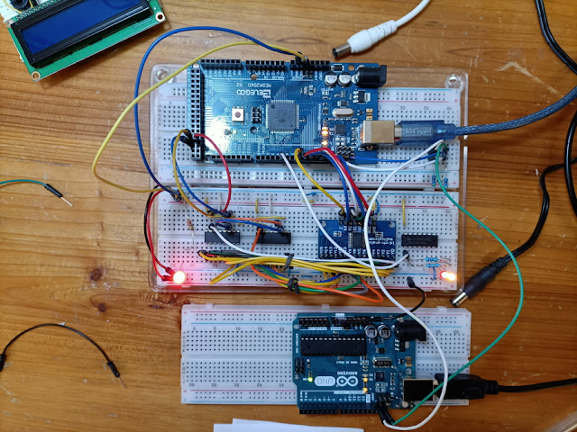
The fully wired circuit is depicted in Figure 7.


Fig. 7

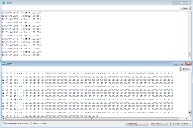
Figure 8 displays the serial monitors of the two Arduino microcontrollers: the data source (top) and the receiver (bottom). Two "COM4" ports are displayed because the Arduino boards are driven by two separate PCs. Note that a very low clock rate was chosen in the firmware implementation allow easy reading of the serial monitors.

Fig. 8:serial monitors output of the two microcontrollers

A note about Bitrate Expansion vs. Datarate Preservation
The integration of the buffer-extender and the hardware multiplexer within this data pipeline serves a dual purpose: expanding the transmission bitrate while strictly preserving the baseline datarate (the actual information payload). 
Bitrate Expansion (50 bps→600 bps): The system ingests a baseline digital signal at 50 bps and up-rates the transmission frequency by a factor of 12, delivering a 600 bps synchronous stream at the final output. This high-speed clocking is structurally required to match the ingestion constraints of the STANAG-4285 modem. 
Datarate Preservation: While the physical signaling speed increases, the net information throughput remains exactly identical to the 50 bps input. The system does not inject new data or alter the original message content. Instead of increasing information capacity, the remaining bandwidth created by the 12x clock multiplier is entirely dedicated to data redundancy. Each original bit is algorithmically mapped across the 12-bit output frame.

https://disk.yandex.com/d/-9xhLnBZ-7RPKw  Royal Australian Navy, 14874.0 kHz CF
https://disk.yandex.com/d/MyzyM20VOnYTvg Portuguese Navy, 12704.5 kHz CF


(1) In professional HF communications (such as STANAG 4285 or MIL-STD-188-110A), the DCE (Data Circuit-terminating Equipment / Modem) acts as the master of the communications link, while the DTE (Data Terminal Equipment / Data Source) acts as a slave regarding timing and throughput.

17 February 2022

5N1 frames To 112-bit period stream (just for fun, again)

This post is the follow up, and the counterpart, of the previous one (112-bit T stream To 5N1 frames, just read it for background). If while receiving we need a "downsampling" by a factor of 16 of the 112-bit period stream coming from the modem, when transmitting we have to expand the source 5N1 frames bitwise by the same factor before to forward them to the modem. As in the "downsampler", I used the multiplexer/demultiplexer module CD74HC4067 and two I2C connected Arduino boards.

Each bit of the 5N1 frames is spread to a 16-bit D-type latch register which is three-state connected to the 16-input of the multiplexer, the inputs are then selected and forwarded to the multiplexer serial output at a speed that is 16 times faster than the 5N1 frames (figs. 1,2).

This way each input bit is 16 times repeated in the serial output and thus the stuf performs the 16x expanding. Not having a 16-bit register at home, I used two 74HC595 (8-bit, serial-in, parallel-out shift register that feeds an 8-bit D-type register).
 
Fig.1 

Fig. 2

The 5N1-112 conversion is not done via software: a board takes care of sending data to the other one which forwards 'em and manages the ICs. Input/output data are dispalyed on the serial ports (COM3 on the sender, COM4 on the receive expander, see figure 3 below).

Fig. 3

As already mentioned in the cited post, I do not  aim to "replicate" the circuit used to perform the 5N1-112 conversion but only try to simulate its operation through the use of a multiplexer. For those interested in playing with the two circuits (...but I really don't think so) the 4 rough "sketches" can be downloaded from here along with the data sheets of the used ICs:   
https://disk.yandex.com/d/SVTcXiikai1VRQ 

11 February 2022

112-bit period stream To 5N1 frames (just for fun)

I recently re-thinked to the odd 112-bit period stream sent by UK MoD via STANAG-4285 and described  here, more than anything else I was intrigued by the "stuff" used for the manipulation of the streams. Looking at the bitstream of figure 1, one can see that either the sync sequence and the Initialization Vectors are 16 times bitwise expanded, thus that "stuff" shall sit in the middle between the crypto device and the STANAG-4285 modem, assuming that it is not embedded or implemented in one of the two devices. 

Fig. 1

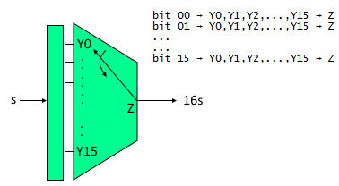
During the receive phase it shall perform a downsampling of the received 112-bit period stream by a factor of 16 while in the transmit phase it will expand the source 5N1 frames bitwise by the same factor: in a few words, in some way the stuff acts like a multiplexer/demultiplexer (figure 2).

Given that:
Z = serial input/output 
Yn = input/output channels

Tx side (expander):
each input bit is applied to all the input channels and their selection speed is 16x the speed of the input bits, ie:
bit 00 → Y0,Y1,Y2,...,Y15 → Z
bit 01 → Y0,Y1,Y2,...,Y15 → Z
...
bit 15 → Y0,Y1,Y2,...,Y15 → Z

this way each input bit is 16 times transferred into the serial output and thus performing the 16x expander.

Rx side (downsampler):
The selection of the output channels is in sync with the input bits (same speed), ie:
bit 00 → Y0
bit 01 → Y1
...
bit 15 → Y15

since all the sixteen bits have the same value (1 or 0), it turns out that draining the output only from Y0 (or from any other single channel) we get the needed downsampling by 16.

Fig. 2

I started thinking about how that "stuff" could be implemented: software or wired-logic solution. The software solution is easy to code and may be based on a PC as well as on Single Board Computers such as Raspberry Pi or Banana Pi or also on microcontrollers as Arduino, obviously the serial interfaces are needed. Just as a Proof of Concept, and  to have some fun, I decided to to demonstrate the wired-logic feasibility with multiplexer/demultiplexer breakout board module CD74HC4067 and two Arduino boards connected via I2C communication bus in the Master-Slave configuration (1). 
 
In the downsampler Rx configuration (figure 3), one Arduino board ("Uno") acts as Slave and it's requested to send the 112-bit period stream, this board represents the output of the S4285 modem; the second Arduino board ("Mega2560") is the master and drives the dmux CD74HC4067:
• requests data to the slave and forwards them to the dmux serial input 
• selects the output channel Yn through the address bus S0-S3
• withdraws the Y0 output and forwards it to a LED (ie the following crypto device)
The master board also controls the HD44780 LCD which is added to display the received 5N1 frames after their downsampling ...almost useless since data are dispalyed on the serial ports (COM3 on the sender, COM4 on the receiver: see figure 5).
 
 
Fig. 3 - Downsamnpler Rx connections


Fig. 4 - downsampler at work

Fig. 5 - serial port monitor of sender (COM3) and dowsampler (COM4)

As aforementioned, this post is not intended to build the conversion circuit 112-5N1 but to simulate its operation through the use of a simple demultiplexer ... and to have some fun. In a next post I will also try the reverse operation 5N1-112 but always using the module CD74HC4067 this time as a multiplexer. By the way, I used the CD74HC4067 as it can be used both as a multiplexer and as a demultiplexer, in this circuit it can be replaced with the SN74154 (dmux only).  


(1) The I2C communication bus is very popular and broadly used by many electronic devices because it can be easily implemented in many electronic designs which require communication between a master and multiple slave devices or even multiple master devices. The easy implementations comes with the fact that only two wires are required for communication. The two wires, or lines are called Serial Clock (SCL) and Serial Data (SDA).  The SCL line is the clock signal which synchronize the data transfer between the devices on the I2C bus and it’s generated by the master device. The other line is the SDA line which carries the data.

17 August 2021

188-110A, D1 D2 patterns and interleaved blocks boundaries (hardware implementation)


As well as to have some fun with ICs, I wanted to implement a part of the 188-110 modem to definitively understand the relationship between the periodicity of its bit stream and the lengths of the scrambler/interleaver (as indeed already discussed in other blog posts). The "core" is the data sequence randomizing generator: a 12-bit LFSR (Linear Feed Shift Register) with the functional "one-to-many" configuration and described by the polynomyal x^12+x^6+x^4+x+1. I implemented that LFSR by using twelve D-type flip-flop and three XOR gates, plus three 8-bit serial-to-parallel shift registers to manage the LFSR initial state; its operation, and other 188-110A modem functions such as clock, symbols formation and scrambler, are controlled by an Arduino board. The part more strictly related to the circuit (logic and electronics) is illustrated in the second part of the post.

That set of wires & ICs works great and my tests mainly concerned the data rate of 2400 bps: at that speed the framing has a duration of  48-symbols: 32 symbols in the UnKnown data position followed by a 16 symbols in the Known data (probes) position. As expected, the period of the bit stream is 480-symbol/1440-bit length (ie 10 frames) and matches exactly  3 runs of the sequence randomizing generator (reset'd every 160 symbol): regardless of the interleaver block length (figure 1).

Fig. 1 - 1440-bit/480-symbol period of the Arduino bit stream

However, there is still an uncertainty about the length of one interleaver block (short or long), or, better, about how it is indicated.
According to MIL 188-110 Standard, when the two Known symbol patterns preceding the transmission of each new interleaver block are transmitted, the symbols of these two Known patterns shall be set to Dl and D2 values, respectively, as defined in table XV of the standard. These two particular symbol patterns are indicated in figures 2,3 respectively for a real-world signal and the Arduino signal (both are 2400bps/Short).

Fig. 2 - D1 D2 patterns in a real-world bit stream

Fig. 3 - D1 D2 patterns in the Arduino bit stream

As you may check, each three rows the patterns of the last two probes exhibit the discontinuity due to the D1 and D2 values: therefore, since that three rows of the 480-symbols period contain 3×10 = 30 frames, the block length consists of 30×32 = 960 tribit symbols for the short interleave setting. The measured value is in constrast with what indicated in the standard; indeed, quoting MIL 188-110B #5.3.2.3.7.1.2,  "[...] The block length shall be 1440 tribit channel symbols for short interleave setting and 11520 tribit channels symbols for the long interleave setting".
You will get 1440 symbols if you consider also the probe symbols, ie if you compute 30×48 instead of 30×32... but the probe symbols are not interleaved, ie they are not fetched from the interleaver matrix! On the other hand, the short interleaver matrix for 2400 bps consists of 40 rows and 72 columns, ie 2880 bit that just will form 960 tribit symbols: this way, one interleaver block coincides with the dimensions of the correspondent intereleaver matrix. A similar calculation can be verified for the long interleave settings.

So, in my opinion, it seems that when 188-110 Sandard talks about the length of one interleaver block, it refers to all(!) the bit that compose UnKnown and Kown data symbols (indeed it talk generically of "channel" symbols) and not to the bit which are actually fetched from the interleaver matrix and that consequently will be used to form the UnKnown data symbols only (as it would seem more logical to me).

Notice that if the sequence randomizing generator is reset to 0xBAD after 80 transmit symbols, the resulting bit stream is 240-symbol/720-bit length (5 frames), ie just the half of the normal operations (as expected!).  

Fig. 4 - 720-bit period (LFSR reset'd after 80 transmit symbols)

Arduino part
As said above, the sequence randomizing generator is a 12-bit LFSR that I implemented by using 12 D-type flip-flops (6 x 74HC74) and 3 XOR gates (74HC86) used for the feedback path. Since the LFSR shall be preload to the initial seed 0xBAD (101110101101), we need to control the async set/reset inputs of the 12 flip-flops, therefore we need to manage 24 pins from the Arduino board and probably we do not have such number of ports available on the board. The idea is to use a serial-in parallel-out shift register (74HC595) to control 8 lines at a time, so link three registers together will give us the chance to get 24 parallel lines by sending 3 bytes on a serial pin of the Arduino board; that way, each 8-bit shift register will drive the set/reset inputs of four flip-flops (figure 5).

Fig. 5 -  three 8-bit shift register used to manage twelve D-type flip-flop

The connections for wiring the preload part are shown in figure 6

Fig. 6
188-110 Standard suggests to implement the sequence randomizing generator using a 12-bit LFSR in the "one-to-many" configuration, ie the most-significant bit is fed back directly into the least significant bit, and is also individually XORed with the other bits 6,4,1 (below in Figure 5). The connections for wiring are shown in figure 7.
Fig. 7
 
The Arduino "sketch" (the software) can be downloadeed from:
https://disk.yandex.com/d/TJvzhdThgCwClA

74HC74 is a dual positive edge triggered D-type flip-flop with individual data (nD), clock (nCP) inputs and asynchronous set (nSD) and reset (nRD) inputs.

74HC86 is a quad 2-input EXCLUSIVE-OR gate. 

74HC595 is an 8-bit serial-in/serial or parallel-out shift register with a storage register and 3-state outputs. Both the shift and storage register have separate clocks. The device features a serial input (DS) and a serial output (Q7S) to enable cascading.

pinning of the used ICs

Hardware (Arduino + breadboard) and software implement the red-circled parts of the 188-110A modem:


3 August 2021

use PuTTY as Arduino monitor for LFSR circuits

Given the lack of really interesting signals on air, at least these days or no luck in hunting, I am playing with the semi-hardware (1) implementation of pseudo-random sequence generators: a way to spend these hot afternoons combining electronics and signal analysis. Waiting for the delivery of the 74xx595 chips, necessary for the 188-110A sequence generator, I wanted to implement a version of the LFSR (Linear Feedback Shift Register) described by the polynomial x^4+x+1 and verify - even if there was no need - its binary sequence. 

So, why a post title about PuTTY? I needed to save the bit stream produced by the circuit for its subsequent graphical representation but unfortunately the Arduino' console (embedded in its development environment) does not allow the content to be saved unless you stop the process and use the copy & paste method, a workaround not always effective in case of output that cause scrolling screen: using PuTTy is just what you need. "Putty" is a free SSH and telnet client for Windows and if it's not yet part of your resources you can quickly download and install it from its site [1]. After launched, select the right serial port number and speed as indicated by Arduino then on the session tab select the printable output and the path of the output file (figure 1): that's all, power-on your circuit and connect Putty, you do not have to run the Arduino environment to get a monitor.

Fig. 1 - configuring PuTTY for use as Arduino' monitor

Fig. 2 - PuTTY at work

Back to the LFSR circuit (four D-type Flip Flop and one XOR gate), its logic is quite simple and does not require much explanation even if I'm not really an artist in wiring the bredboards (figs. 3,4). Just notice that I use the Arduino MEGA 2560 so if you do not use such board you will have to change the input/output pins 6 (preset/clear), 8 (clock), 10 (Q1), 11 (Q2), 12 (Q3), 13 (Q4) by editing the sketch [2] according to your choices. Mind you that the clocking speed is exaggeratedly low to allow both the set of  the initial state of the registers (see below) and an easier reading of the monitor.

Fig. 3

Fig. 4

As said, the LFSR is described by the primitive polynomial x^4+x+1, i.e. its sequence is termed as m-sequence (maximum-length sequence) and has a length T = 2^n -1, where n is the number of the used registers (also termed as "stages"); in this case the LFSR employes four registers thus produces a 15-bit length sequence that repeats itself over time. Storing the "state" of each register (outputs Q1, Q2, Q3, Q4) we get 4 × 15 = 60-bit length pattern (figure 6).
Notice that the 0000 state is never crossed since in that state the sequence simply does not start, the registers are as stuck in that state; therefore, the 0000 state is never used as initial state (or "seed") of the LFSR. To start the state' cycles and set the seed to 1000, you will need to keep pin2 HIGH just for a clock positive transition, ie simply wire pin 2 - the data input of the first register - to the +5 V line of the bredboard, clock pulses are monitored by the LED in figure 4. 

Obviously, the same sequence will be obtained by simulating the LFSR using an Octave script (LFSRv2.m) [3] or the Logic Simulator App [4] [5] or the LFSR Testbench too [6]: you have many tools at your disposal.

Fig. 5 - LFSR states output logged by PuTTY and states output produced by Octave script

Fig. 6 - the 60-bit patterns generated by the four states of the LFSR

The sequences in figures 5-6 are obtained implementing the "many-to-one" feedback structure but you could also implement its "one-to-many" counterpart (2): in which case the sequence of the states will be slightly different (!) though the initial states are the same (figure 7).

Fig. 7 - many-to-one and one-to-many feedback structures for x^4+x+1 LFSR

«A way to spend these hot afternoons combining electronics and signal analysis» I said... yep, but the beach is much more better! 

(1) semi-hardware since some features such as the clock are software implemented 

(2) in "one-to-many" configuration there is never more than one level of combinational logic in the feedback path, irrespective of the number of taps being employed in the traditional "many-to-one" configuration (increasing the levels of logic in the combinational feedback path can negatively impact the maximum clocking frequency).

[1] https://www.putty.org
[2] https://disk.yandex.com/d/U4rXrZ7JWWgAGQ
[3] LFSRv2.m Octave script https://disk.yandex.com/d/jOX64f8u19jYFw
[4] Logic Simulator project https://disk.yandex.com/d/UcLU_1eAwtubXA
[5] Logic Simulator Apk https://logic-circuit-simulator-pro.it.aptoide.com/app
[6] https://disk.yandex.com/d/hMe696WAWjth8Q


26 July 2021

playing with Arduino and a 12-bit LFSR


The circuit is just a test of the operation of the 12-bit LFSR x^12+x^6+x^4+x+1 used in 188-110A serial tone modems, in view of its full implementation; its software simulation has already been seen in a previous post, to which I refer for further insights. The 12 flip-flops and the 3 XOR gates implement the "one-to-many" configuration, according to the 188-110A standard. Since the 74xx374 does not provide the asynchronous preset / clear inputs, the LFSR is a "free runner" that is, it is not reset to a certain initial state (seed) after n-cycles; therefore all the circuits related to loading the initial pattern (0xBAD) are missing. 

Pinning and logic circuit (connections) are shown in figure 2: the electric connections (+/- 5V power) are omitted, the connections to the pins of the Arduino board are indicated (notice I used AT MEGA 2560 board so you had to change connections and code in case you use a different board).

Fig. 2 - logic connections and pinning

The 220 ohm resistor & the blue led visible in the photo on the clock line, are not reported in the circuit, they just show the clock pulses... obviously in case of a very low clock speed.

The code of the sketch is quite simple, I just used a random number generator to simulate symbols 0-7 from Modified-Gray Decoder (MGD) and a 8x8 array to perform the scrambler: the tribit number supplied from the random number generator is modulo 8 added (mod8[LFSRsymbol][randSymb]) to the three bit value supplied by LFSR (pins 53,51,49). Results are written into a buffer which is then sent to the serial port (figure 3).

Fig. 3


The 74HC374 is an octal positive-edge triggered D-type flip-flop with 3-state outputs (the second 74HC374 is half used, ie it provides only 4 flip-flops). The device features a clock (CP) and output enable (OE) inputs. The flip-flops will store the state of their inndividual D-inputs that meet the setup on the LOW-to-HIGH clock transition. A HIGH level on OE causes the outputs to assume a high impedance OFF state (OE input does not affect the state of the flip-flops). The74HC86 is a quad 2-input EXCLUSIVE-OR gate used to form the feedback chain.

https://disk.yandex.com/d/7gestYtENRF6VQ

13 November 2020

a new toy

Just bought (and alreday at home) the compatible Arduino™ Mega 2560 R3  board: a microcontroller board based on the ATmega2560. It has 54 digital I/O pins (14 of which can be used as PWM outputs), 16 analogue inputs, 4 UARTs (serial hardware interfaces), a 16-MHz crystal oscillator, a USB interface, a power connection, an ICSP header and a reset button.

Really hope to do something useful with it for signals and analysis, as well as fool the time during covid-19 lockdown.